


Key Steps
HieFo's InP fab enables us to provide specialty chips for next-generation telecom, data center, optical sensing applications.

DEVICE DESIGN

EPITAXIAL CROWTH

WAFER PROCESSING

COB SUB-ASSEMBLY
Wafer Fab Introductions
HieFo owns and operates a world-class InP semiconductor wafer fabrication plant at our corporate headquarters. The state-of-the-art facility supports the development and manufacturing of best-in-class Telecom wireless, Data Center and optical sensing market.
Our vertically integrated fabrication facility is equipped with state-of-the-art MOCVD reactors for wafer processing of InP-based devices, including lasers, APDs, and PIN photodetectors. The plant also houses advanced equipment such as steppers, wafer tracks, ICP and RIE systems, diffusion furnaces, metal and dielectric deposition tools, as well as cleaving and dicing stations. Our comprehensive process flow encompasses MOCVD epitaxy, wafer processing, facet coating, chip processing, and laser diode assembly.
Supported by a highly experienced technical team with deep expertise in device design, epitaxial growth, wafer fabrication, device characterization, and chip-on-block (COB) sub-assembly, we deliver high-performance products from initial development through full-scale manufacturing. We are able to partner with our customers from the earliest stages of development to identify cost drivers and deliver custom optical solutions optimized for their specific applications. Our extensive experience and flexible manufacturing enable rapid turnaround of prototypes and bespoke components.
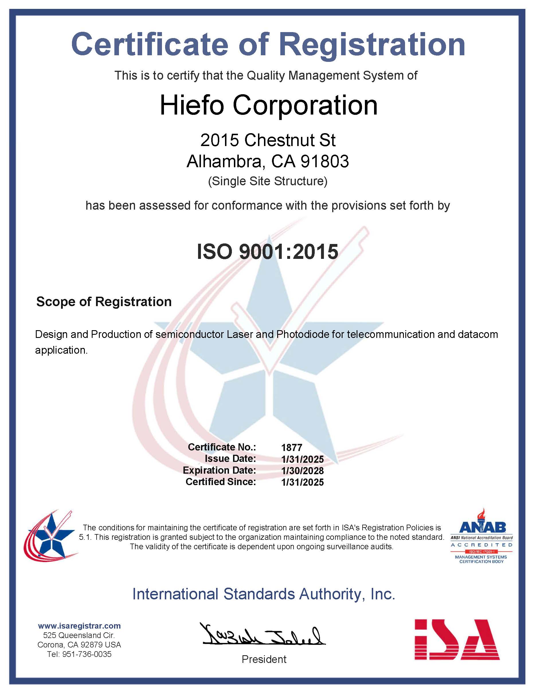
We are proud to announce that HieFo has achieved ISO 9001 certification, demonstrating our commitment to quality management and continuous improvement in all aspects of our operations. This certification reflects our dedication to providing consistently high-quality products and services to our customers.


ONLINE INQUIRY
Contact Semtech Sales & SupportCOMPLETE YOUR JOB APPLICATION
View Careers at Semtech